Dr. Rudy Schlaf's Group_____________________________________________________
Department of Electrical Engineering - University of South Florida
Last Modified Aug 2013
(c) Rudy Schlaf
Webmaster
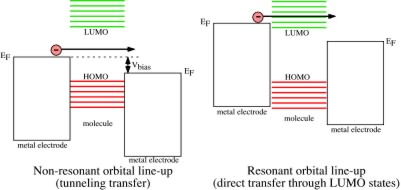
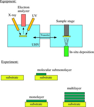
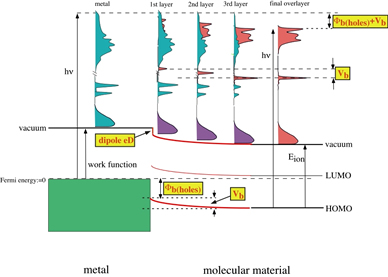
Electronic and Chemical Structure of Macro-Molecular Interfaces: Macro-molecular materials such as luminescent polymers, bio-molecules (DNA, proteins), or inorganic nano-clusters have many promising applications in devices ranging from molecular transistors to pathogen sensors. Integration of these materials in devices requires a thorough understanding of their interaction with other materials such as substrates or electrodes. For example, when it comes to charge transfer through a single molecule, the injection barrier between highest occupied and lowest unoccupied molecular orbitals (HOMO, LUMO), and the contacting electrodes decides between tunneling and resonant charge transfer (Fig.1) Our current research focuses on the investigation of interfaces (contacts) of macro-molecular materials with inorganic materials (Au, graphite, Si etc...), that can be used as electrodes or supports in actual device structures. These experiments are performed using photoemission spectroscopy (PES) in combination with electrospray in-vacuum deposition of the macro-molecular materials of interest (see tutorials for details). In a typical experiment to investigate the interface between a macro-molecular material MM and an inorganic material IO, a substrate composed of IO would be inserted into the PES vacuum system, cleaned and characterized. Then, without breaking the vacuum, MM would be deposited in several steps, typically starting at submonolayer coverages, and then continuing up to several monolayers thickness (Fig.2). In between deposition steps, the surface is characterized with PES and a series of spectra is obtained as shown schematically in Fig.3. This set of spectra gives detailed insight into the electronic structure of the interface, as well as the chemical make-up of the interface region. The typical endresult is an orbital line-up diagram, showing the charge injection barriers between IO and MM. This information can for example be used to select an appropriate substrate/electrode material combination enabling good charge injection in to the MM, while avoiding damaging interface reactions (which would degrade the device) etc... |
Fig.1: Orbital line-up between molecule and electrodes.
Fig.2 Experiment schematic: Two chamber set-up enables transfer between deposition and analysis without exposure to the ambient. This allows to build up the interface in several steps while characterizing the electronic/chemical structure in between without interference of contamination.
Fig.3: Orbital line-up determination from series of PE-spectra. |


